
Thin-Film Technology
Enabling the Next Generation of Semiconductor Devices
Thin-film technology is a key enabler of next-generation semiconductor devices. From transistors and sensors to advanced packaging, precisely engineered thin films improve performance, energy efficiency, and reliability.


Thin-film technology is one of the fundamental building blocks of modern semiconductor manufacturing. Ultra-thin layers of conductive, insulating, and functional materials enable the performance, miniaturisation, and reliability of microchips, sensors, power electronics, photonic devices, and advanced electronic systems.
Nearly every semiconductor device relies on thin films to achieve the precision and functionality required for today’s technologies.
As conventional transistor scaling approaches its physical limits, innovation increasingly depends on advanced thin-film materials and deposition processes. Technologies such as Atomic Layer Deposition (ALD), Chemical Vapor Deposition (CVD), Physical Vapor Deposition (PVD), and precision metrology enable the development of next-generation semiconductor architectures, advanced packaging, and high-performance electronic devices.
Nearly every component in a chip relies on thin films: the gate dielectrics in transistors, the metal interconnects that wire components together, the barrier layers that prevent unwanted diffusion between materials, and the passivation layers that protect the finished device.
As transistors have shrunk toward the atomic scale, controlling these films with atomic-level precision has become essential for device performance.
As chips move toward more complex 3D architectures, advanced packaging, and novel materials (high-k dielectrics, 2D materials like graphene, new low-resistivity metals to replace copper at small dimensions), thin-film deposition and metrology techniques continue to evolve in tandem, often representing some of the most capital-intensive and technically demanding equipment in a fab.
At AT-C³, we support companies throughout the entire thin-film innovation process. By combining research excellence with industrial expertise, we help accelerate the transition from laboratory-scale innovation to reliable, market-ready semiconductor solutions.

Methods & Competencies Driving Thin Film Innovation
Thin-film technologies are fundamental to modern semiconductor devices, enabling higher performance, greater efficiency, and increased reliability. AT-C³ supports companies with expertise in thin-film deposition, characterisation, process optimisation, and advanced packaging – accelerating innovation from research to industrial application.
Thin Film Deposition
Thin-film deposition forms the foundation of modern semiconductor manufacturing. AT-C³ supports the development and optimisation of deposition technologies that enable high-performance microchips, sensors, photonic devices, and advanced electronic systems. Our expertise spans a range of deposition processes, including Physical Vapor Deposition (PVD), Chemical Vapor Deposition (CVD), and Atomic Layer Deposition (ALD), helping companies develop reliable and scalable solutions for industrial applications.
We support you at every stage
From feasibility to optimization – our tech services guide you through every phase of your product journey.
AT-C³ can help users explore the potential benefits of using in-house developed chips in products and evaluate the costs involved in such development. Examples may include replacing a PCB with standard components using an in-house developed integrated circuit (ASIC). This study could also examine alternative manufacturing processes to optimize an existing ASIC. Feel free to contact AT-C³ if you’re interested in learning more about a potential feasibility study for your company.




Request the service catalogue to discover the full potential
Use our submission form to bring your innovation to AT-C³ – we’ll support you from concept to realization.
Get to know more focus areas





Inside Austria’s Chip Industry

10. September 2026
AT-C³ at FFG Forum 2026: Strengthening Austria’s Innovation and Technology Ecosystem
At the FFG Forum 2026 in Vienna, AT-C³ was represented by Lukas Lassbacher, who introduced the Austrian Chips Competence Center and represented its role within the European semiconductor and innovation ecosystem.
More


27. August 2026
Free Online Training Courses in the microelectronics field starting in October!
AT-C³ is officially launching its new training program in October 2026, offering free online courses for professionals, researchers, students and anyone interested in deepening their knowledge of microelectronics.
More
14. July 2026
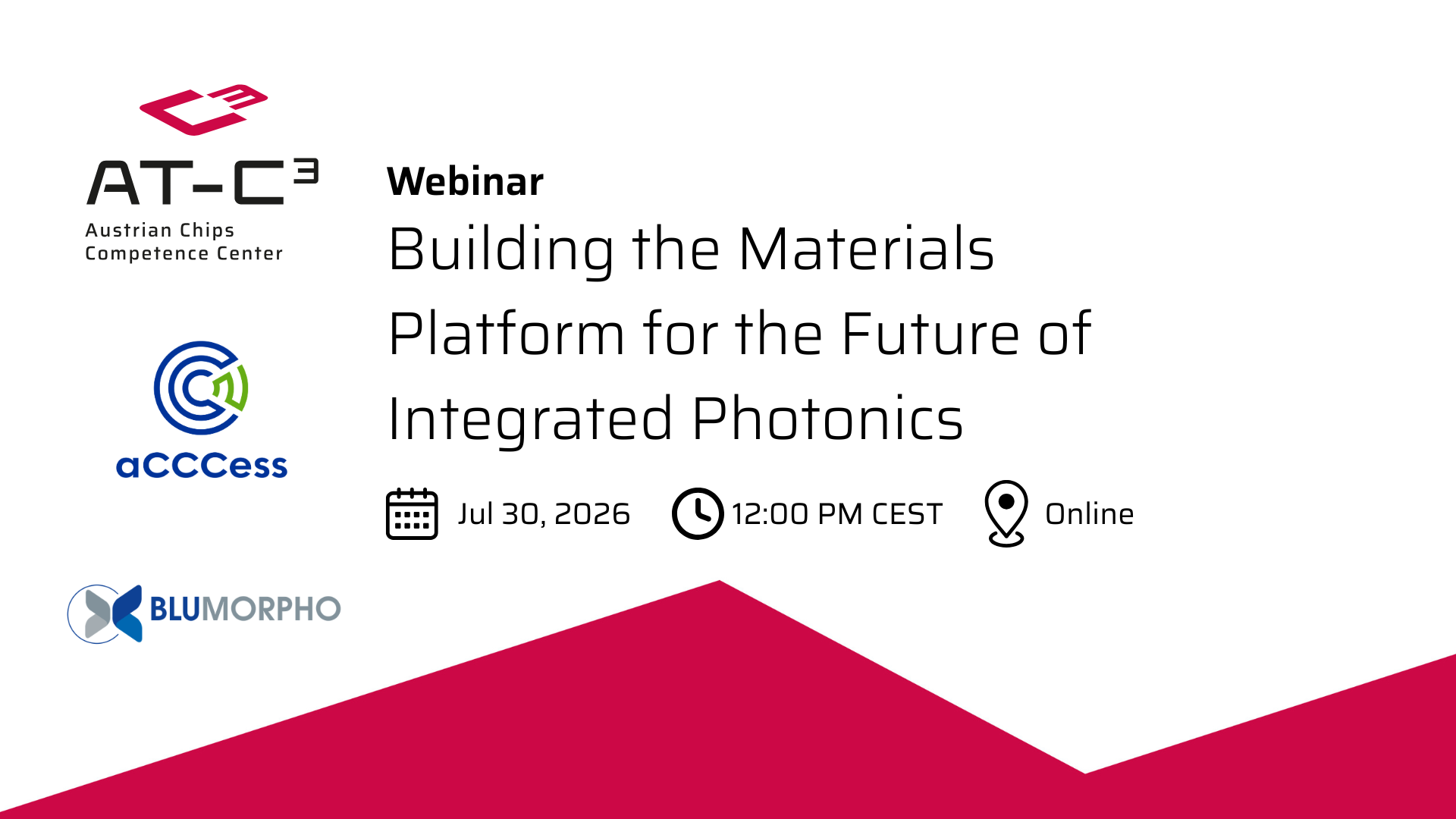
Webinar 30 July 2026: Building the Materials Platform for the Future of Integrated Photonics
In this Chips Think Tank webinar on July 30, 2026, Jean-Louis Guyaux, VP Technology at Riber, will share how one of Europe’s leading epitaxy equipment manufacturers is evolving from supplying MBE systems to enabling complete materials platforms for integrated photonics.
More