
ADVANCED MATERIALS SEMICONDUCTOR PRODUCTION
Driving material innovation
We help companies develop and apply next-generation materials by combining expertise in modeling, simulation, synthesis, and analysis – with a strong focus on sustainability and collaborative innovation.

Advancing material innovation through integrated expertise in modeling, simulation, synthesis, and analysis – with sustainability at the core.
The development and application of advanced materials with improved properties rely on a network of interconnected disciplines: modeling, simulation, synthesis, analysis, and innovation. Synthesis can be performed independently or at partner sites, enabling flexible collaboration and the integration of diverse competencies. Sustainability is a guiding principle throughout – from material selection to production environments and end-use applications – ensuring solutions that meet both technological and environmental goals.
Advanced materials are increasingly central to keeping microelectronics progress on track, especially now that simply shrinking transistors is no longer enough to deliver the performance, power, and density gains the industry has historically relied on. A brief tour of the main categories:
Silicon carbide (SiC) and gallium nitride (GaN) have moved from niche to mainstream in power electronics. They handle higher voltages, switch faster, and operate at higher temperatures than silicon, which is why they appear in EV inverters, fast chargers, and data center power supplies.
As Moore’s Law scaling slows, much innovation has shifted to packaging: glass-core substrates, advanced underfills, low-loss dielectrics for high-frequency signaling, and novel thermal interface materials to manage heat in increasingly dense 3D-stacked chips.
Looking further out, materials such as superconductors, topological insulators, and phase-change materials (used in memory and neuromorphic devices) are being investigated for entirely new computing paradigms beyond traditional CMOS.

Methods & competencies driving material innovation
Advanced materials are shaping the future of semiconductors and electronic systems. As conventional scaling reaches its limits, new materials and manufacturing technologies are driving higher performance, greater efficiency, and enhanced reliability. AT-C³ supports companies in developing, testing, and validating innovative material solutions, from power electronics to next-generation computing technologies.
Sustainable Materials
SUSTAINABLE MATERIALS
Evaluates and verifies the effects of materials in production, use and recycling on environmental compatibility, sustainability and availability. Development and application of new materials with improved properties in sustainability. The materials are developed based on ecodesign and predictive life cycle analysis and can be examined for, e.g., biodegradability.
What you gain
- Durable and low-maintenance materials
- Securing raw material availability through recycling
- Building material cycles
- Energy-efficient production processes
- Use of renewable raw materials
- More sustainable materials and material-based products
- New circular products
- Innovative material development based on eco-design guidelines
- Regulatory compliance (e.g., REACH – chemicals; eco-design guidelines, etc.)
- Marketing advantage through sustainability
- Cost-effective manufacturing through additive manufacturing
Why it pays off
- Safe, future-proof material selection
- Substitution of critical or environmentally harmful materials
- Life cycle analysis for assessing environmental impacts
- Reduction of energy and material consumption in production
- Reduction of harmful substances
- Provide basic knowledge about eco-design and sustainability, as well as environmental cost-benefit analysis
We support you at every stage
From feasibility to optimization – our tech services guide you through every phase of your product journey.
AT-C³ can help users explore the potential benefits of using in-house developed chips in products and evaluate the costs involved in such development. Examples may include replacing a PCB with standard components using an in-house developed integrated circuit (ASIC). This study could also examine alternative manufacturing processes to optimize an existing ASIC. Feel free to contact AT-C³ if you’re interested in learning more about a potential feasibility study for your company.



Request the service cataloge to discover the full potential
Use our submission form to bring your innovation to AT-C³ – we’ll support you from concept to realization.
Get to know more focus areas




Inside Austria’s Chip Industry
10. September 2026
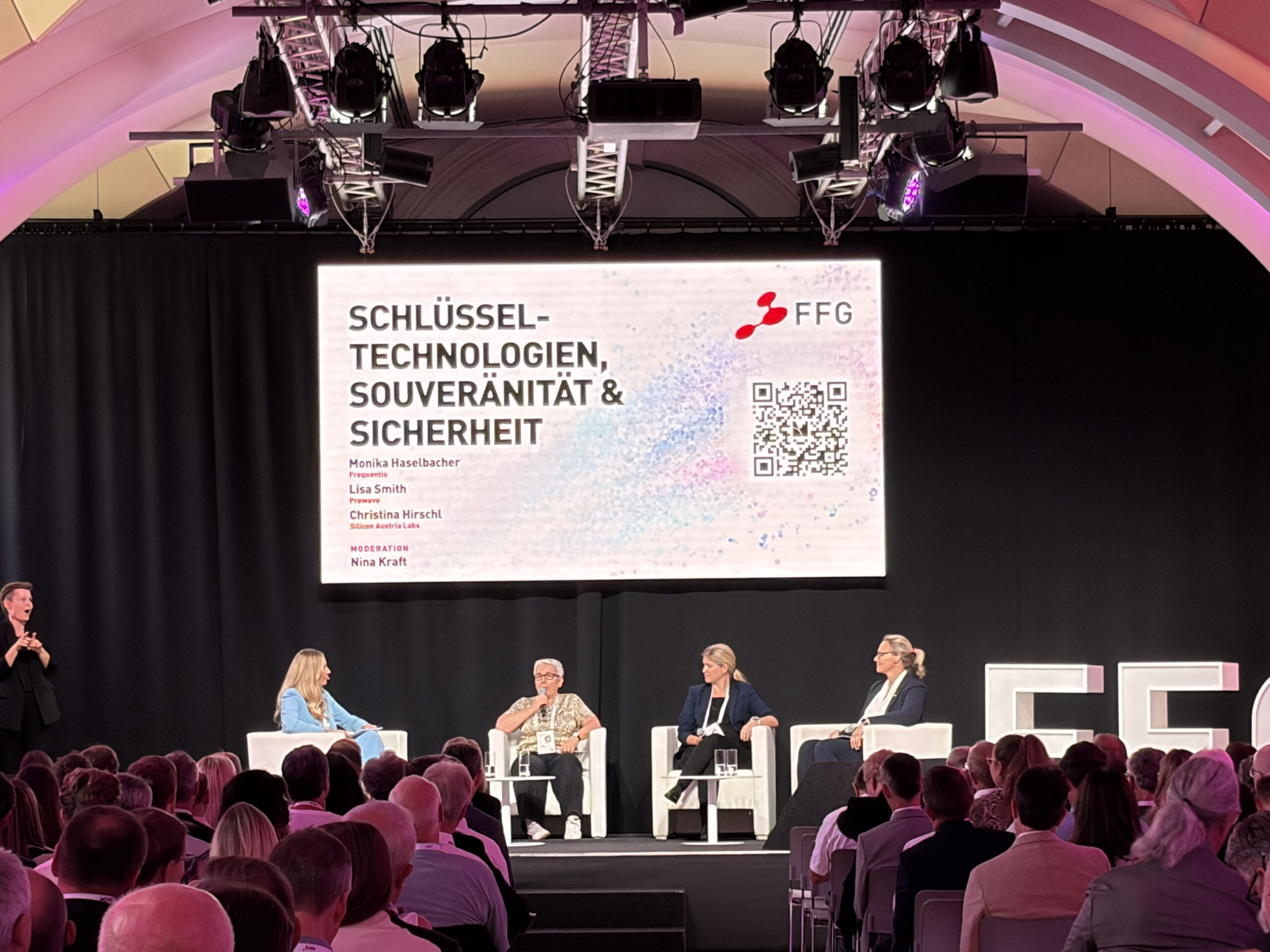
AT-C³ at FFG Forum 2026: Strengthening Austria’s Innovation and Technology Ecosystem
At the FFG Forum 2026 in Vienna, AT-C³ was represented by Lukas Lassbacher, who introduced the Austrian Chips Competence Center and represented its role within the European semiconductor and innovation ecosystem.
More

27. August 2026
Free Online Training Courses in the microelectronics field starting in October!
AT-C³ is officially launching its new training program in October 2026, offering free online courses for professionals, researchers, students and anyone interested in deepening their knowledge of microelectronics.
More
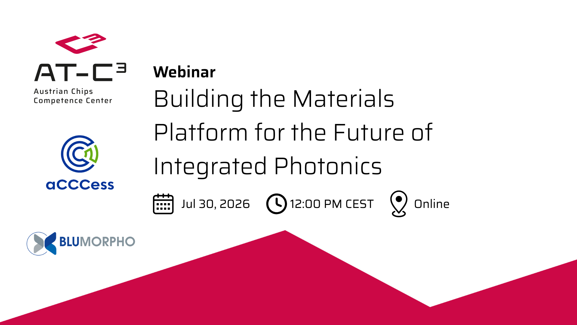
14. July 2026
Webinar 30 July 2026: Building the Materials Platform for the Future of Integrated Photonics
In this Chips Think Tank webinar on July 30, 2026, Jean-Louis Guyaux, VP Technology at Riber, will share how one of Europe’s leading epitaxy equipment manufacturers is evolving from supplying MBE systems to enabling complete materials platforms for integrated photonics.
More